PCB Design and Layout
Understanding electrical parameter requirements
The result can only be achieved if we know what the requirements concerning each component are, as well as how they couple with each other. Going to the basics as to what type of capacitors, resistors, inductors and protection circuitry we need is crucial.
Block diagram
Done by free hand, this part of the process gives a bigger picture of the overall function and communication between major parts of the whole system. The direction of communication between as well as the rating of the components can be specified here. A flowchart-kind representation can be made pointing out the prioritized zones on the board.
Schematic design
Creating the schematics from the scratch is the most important part of the design. Here the symbols of the components are chosen and placed in the work sheet, then electrical connections are made manually, nets are created and pin labels written. After completing the schematics an ERC (Electric Rule Check) is run. Missing connections, short circuits and many other errors are detected by the ERC. Having a non-working board is a taboo at our work
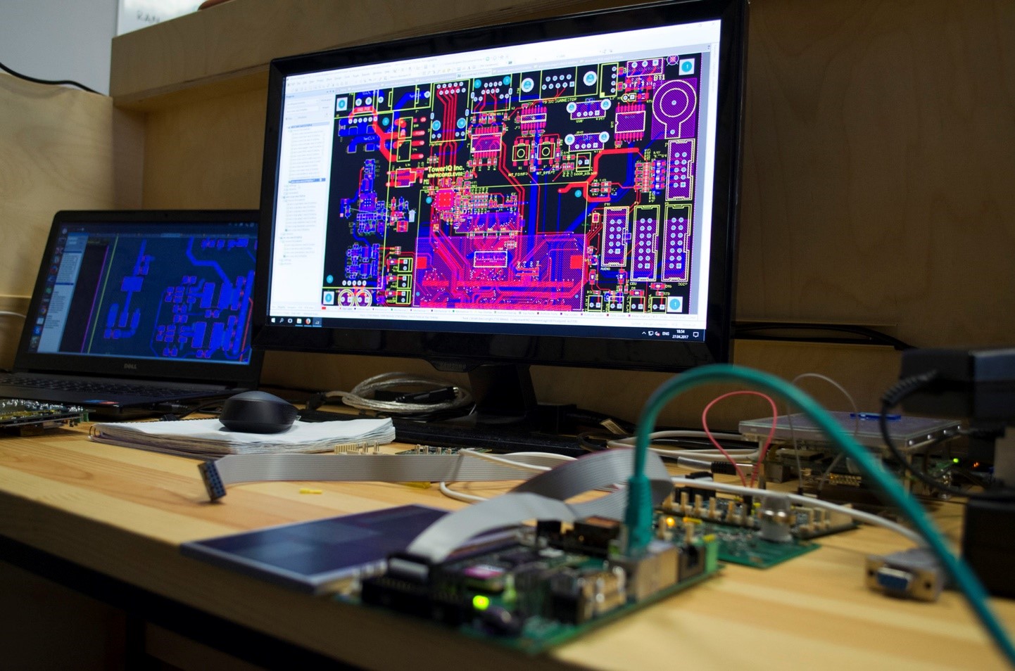
PCB Layout
Once the schematic is ready, the netlist created and footprints are assigned to each component symbol we have to put them in the right place on the board. The board outline is drawn and components are grouped around a central component, so we end up with sections on the board according to their function. Analog components are grouped together, the MCU with the capacitors and resistors around his pins forming another and so on. Via stitching and shielding contributes to the overall performance as well. Proper routes are drawn of different size and type. Copper pouring is also done mainly comprised of nets of power types: GND, Vcc, 3V3 etc.
PCB design simulation testing
Using various Spice software we are able to test the printed circuit board beforehand. Wires to close bring up to noisy signals, increased impedance or worst cases. Signal integrity is a major concern when creating multilayer boards as the current return paths travel along adjacent board layers. To have this in control we run multiple tests, as well as tests concerning the temperature ratings to avoid components failures.
Technical support
We design multilayer PCBs implementing high-frequency digital technology for networking systems and telecommunications. Carefully selected components as a result of thorough schematic study and optimized layout meeting the requirements of the product. Through simulation software, the design is being tested and temperature and impedance checks are done before we give you a PCB ready for manufacturing. Wireless, Bluetooth and other on-board interfaces are highly compatible with the enclosure of the final product, where the position of the buttons, lights, slots and ports are being taken care of, offering you an easy and self intuitive use of the product.